Reveal the key technology of Micro LED, how to achieve acceleration?
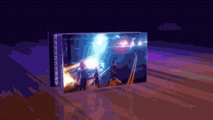
Today, display has become one of the main channels of information transmission, mobile phones, VR/AR devices, wearable devices, vehicle display, tablet/computer display and laser projection are important application scenarios of new display technology.
picture
Among them, the development and industrialization of Micro LED technology has been promoted rapidly, and market opportunities have been increasing, attracting many enterprises to enter and speeding up the reconstruction of the industrial pattern. Micro LED This new star seems to shine especially brightly in 2024.
- What is Micro LED
picture
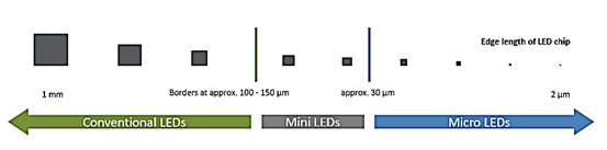
Micro LED English full name is Micro Light Emitting Diode, Chinese called micro light emitting diode, can also write μLED.
Micro-LED, as the name suggests, is a particularly small LED.
Its size is equivalent to 1/10 of the human hair, with no backlight, high photoelectric conversion efficiency, brightness greater than 105 cd/m2, contrast greater than 104: 1, the response time is at the ns level and other characteristics, is the LED film, miniaturization and array, so that its volume reaches only 1% of the size of the mainstream LED, and the pixel distance reaches from millimeter to micron.
picture
The display mode of the Micro-LED is to connect the 10-micron scale LED chip to the TFT driver substrate, so as to achieve the precise control of the luminance of each chip, and then realize the image display.
Micro LED display is the bottom with a normal CMOS integrated circuit manufacturing process to make the LED display driver circuit, and then use MOCVD machine to make LED1 array on the integrated circuit, so as to achieve the micro display, that is, the miniature version of the LED display.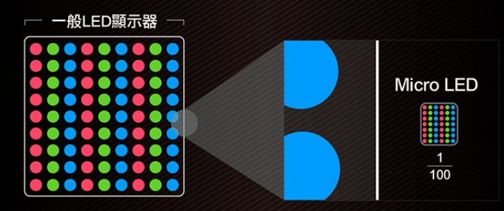
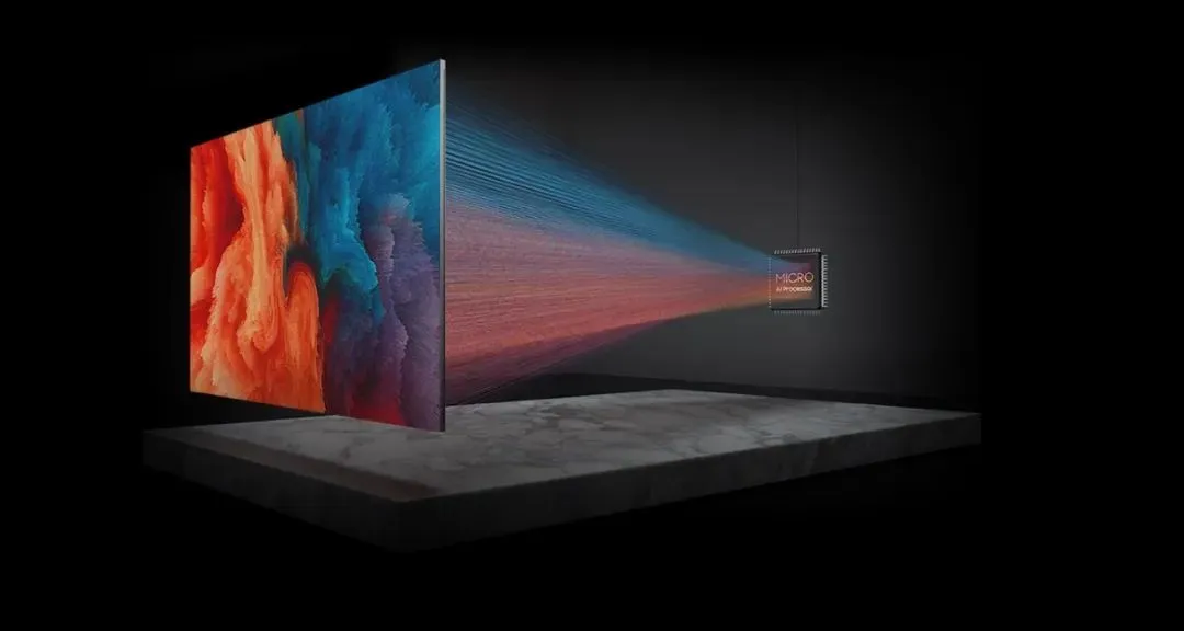
Second, Micro LED display principle
picture
Micro-led is the LED structure design for thin film, Micro, array, its size is only about 1-100μm grade;
After the Micro-LED is transferred to the circuit board in batches, the substrate can be hard, soft transparent or opaque substrate;
By using the physical deposition process to complete the protective layer and the upper electrode, the upper substrate can be packaged and a simple Micro-LED display can be completed.
picture
Three, Micro LED and traditional LED manufacturing process differences
picture
For the process of Micro-LED, many people believe that experience can be learned from traditional LED screens. However, Micro-LED and traditional led display products are very different. Compared with the traditional LED display, the difference between Micro-LED is mainly:
1, the precision of tens of times increased;
- The integration process has changed from in-line insertion, table mounting, COB packaging, etc., to “huge micro-transfer”;
3, defect repairability is almost zero; - The backplane has changed from a printed circuit board to a TFT substrate used for LCD and OLED displays, or a monocrystalline silicon substrate used for CPU and memory.
In short, compared with traditional LED displays, Micro-LED is different in every aspect such as grain, packaging, integration process, backplane, and drive.
Four, Micro LED manufacturing core technology
picture
The core technology of Micro LED manufacturing lies in micro process technology and large volume transfer technology.
Microfabrication technology refers to the length of the original LED chip in the millimeter level after microshrinking to about 1~10μm. Its main requirement is the uniformity of the drive current across the entire wafer wavelength and low defect density.
Most of the previous LED sizes were 10~30mil, that is, 250~ 750μm, and the minimum size of a single chip was 100μm.
And through the micro process technology can break this limit setting, the industry assessment, indoor use of the display size to do at least 5μm, the current LED chip size industry water has generally reached 50μm, Apple is strong, has been able to do 10μm level, Mikro Mesa laboratory has been able to make 3μm size size.
picture
1, LED crystal film, miniaturization, array – micro process technology
At present, the process of semiconductor and chip miniaturization has reached its limit, and there is still considerable room for growth in manufacturing miniaturization. For Micro-LED process, it is mainly divided into three categories: Chip bonding (chip-level welding), Wafer bonding (epitaxial level welding) and Thin film transfer.
(a) Chip bonding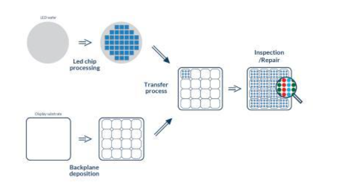
The LED is directly cut into micron-grade Micro LED chip(including epitaxial film and substrate), and the micron-grade Micro LED chip is connected to the display substrate one by one using SMT technology or COB technology. The advantage is that the transfer interval can be adjusted, but it does not have the capacity of batch transfer.
(b)Wafer bonding (epitaxial grade welding)
Using inductively coupled plasma ion etching (ICP) on the epitaxial film layer of the LED, a Micro-LED epitaxial film structure is directly formed, and the fixed spacing of this structure is the required spacing of the display element, and then the LED wafer (including epitaxial layer and substrate) is directly bonded to the drive circuit board, and finally the substrate is peeled off by physical or chemical mechanism. Only 4~5μm Micro-LED epitaxial film structure is left to form a display element on the drive circuit board. The advantage is that it has the ability to transfer in batches, but it can not adjust the transfer spacing.
(c)Thin film transfer (C)Thin film transfer
Physical or chemical mechanism is used to peel off the LED substrate, a temporary substrate is used to carry the LED epitaxial film layer, and then inductively coupled plasma ion etching is used to form a Micro-LED epitaxial film structure. Alternatively, inductively coupled plasma ion etching is used to form micrometer level Micro-LED epitaxial thin film structure.
A physical or chemical mechanism is then used to peel off the LED substrate, and a temporary substrate carries the LED epitaxial film structure.
Finally, according to the required pixel spacing on the drive circuit board, the Micro-LED epitaxial film structure is transferred in batches by using a selective transfer fixture, and the display element is formed by linking to the drive circuit board.
This method has low cost, unlimited display substrate size and batch transfer ability.
2, batch transfer to circuit board – large transfer technology
Micro-LED can essentially be seen as the LED device hundreds or even thousands of times smaller, so that more and smaller Micro-LED light integrated on the same area of the chip. Therefore, the technical bottleneck of achieving Micro-LED in industry lies in this.
This involves a difficult process that almost no other electronics industry uses – “massive micro-transfer” (also known as massive transfer) technology.
What technology is “mass transfer”? Simply put, on the fingernell-sized TFT circuit board, according to the necessary optical and electrical specifications, the number of uniform welding reaches hundreds of thousands, or even more red, green and blue LED micro-grains, and the allowed process failure rate has extremely demanding requirements.
picture
Only a product that achieves such a degree of process can be truly applied to the actual product.
Depending on the final application scenario, the Micro LED can directly produce high-resolution display on Si, GaN or Sapphire substrates for VR and other products, or assemble the Micro LED chip on a larger substrate with logic circuit through mass transfer after production on the substrate. To meet the needs of large-size display applications such as mobile phones and TVS.
Compared with the tiny screen size in AR, VR and other application scenarios, the screen size on mobile phones, tablets and TVS is larger. If you want to use Micro leds in these scenarios, the LED device needs to be separated on the substrate and assembled on a larger substrate:
(1) Only the assembly of the LED is carried out on the substrate with the drive circuit to complete the production of the display screen. Common practices include assembling the LED on a substrate with a TFT, or separately assembling the LED and drive chipset on a glass substrate. The theoretical yield of this technique is low because there are many steps.
(2) The LED and CMOS are integrated so that each unit has its own driver, and then assembled on a larger base. Each structural unit has its own drive, which theoretically improves yield and reduces subsequent repair processes.
picture
Assembly techniques for different applications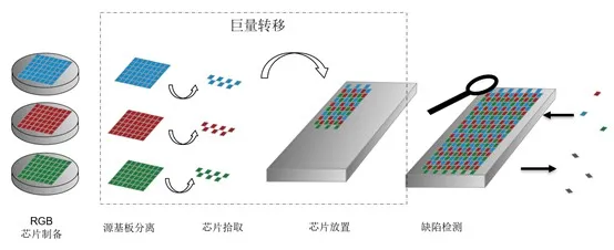
The Micro LED grown on the sapphire substrate needs to be transferred to the glass substrate, which needs to be transported several times due to the size mismatch. The technical difficulty of multiple transfers of micro-devices is particularly high, and it is even more difficult to use products in the pursuit of high-precision displays.
Large volume transfer technology is the core technology in the manufacturing process of Micro LED, and it is also the key to reducing costs. Many companies are developing Mini LED, because the huge transfer technology limits the development of Micro LED. From the perspective of technology iteration, Mini LED is similar to a transition, Mini LED is better than OLED, and Micro LED is better than Mini LED.
Compared with traditional LED display devices, the new Micro-LED is reduced from the original typical size of 300-1000 microns to 1-100 microns, so that it can obtain a higher number of integrations on the chip of the same area. Due to the self-luminous display characteristics of LED, the photoelectric conversion efficiency of Micro-LED is greatly improved, and low energy consumption or high brightness display design can be achieved.
Therefore, Micro-LED has high resolution, low power consumption, high brightness, high contrast, high color saturation, fast reaction speed, thin thickness, long life and other characteristics, and power consumption can be as low as 10% of LCD and 50% of OLED, which is the next generation of display technology expected by the industry.
picture
In the short term, the Micro-LED market is focused on ultra-small displays.
In the medium and long term, the application field of Micro-LED is very wide, across wearable devices, large indoor display screen outside, head-mounted display (HUD), head-up display (HUD), car taillight, wireless optical communication Li-Fi, AR/VR, projectors and other fields.
At present, the AR/VR market is gradually expanding, and looking forward to the future, the key applications of Micro LED fall in the field of AR glasses and vehicle display. Compared with the LCD, LCOS, DLP, LBS, and Micro OLED display technologies commonly used in AR glasses, Micro LED has the characteristics of high pixel, high brightness, high color purity, and low energy consumption. In addition, Micro LED can make the optical unit smaller and maintain high display performance without affecting the appearance of glasses.
The industrialization of Micro LED display technology is accelerating, and various innovative applications are gradually expanding to micro display, consumer electronics, commercial display and other fields.